PCB Design : Some Insights
Introduction
I always knew I had a gap in electronis. Before geting into FPGAs and ASIC deisgn, I was a mechanics enthusiats for most of my teenage years, thus my 1st degree in mechanical engineering (Yeah I’m flexing lol).
When I got into FPGA after digging into an hckathon rabbit hole back in late 2023, I started gainning lots of skills in the fiels but always knew my electronics skill were too off, leading to lack of understanding of PCBs and analog systems.
So I desided to cloase that gap by starting various projects (no spoils ;p) and one of them being to start with a simple PCB design.
Phil’s Lab tutorial
As eexplained in the video embedded above, I decided to floow a phil’s lab tutorial on KiCad9 bt this tutorials any major flaws:
- Displayed Debug Solution are genuinly bad (huge footprint) and expensive.
- Phils forgor to ties the I2C adress pin selector on the I2C Sensor (temporarly fixable post-prod by adding “discovery” in software)
- Sofware is not coverde… at all.
In retrosective, these flaws are not flaws but strengths as they push you, the serious tutorial follower, to find alternatives which pushes a bit further than just dumbly recreating the design and not learning anything at all.
The solutions are described in the video.
The Design
The design is super simple:
- Active system components
- MSPM0 @80Mhz MCU
- I2C accelerotmeter
- USB to UART
- Misc
- ESD protection
- USB C ports (soldered manually just the love of the game)
- 5V to 3.3V
- Crystal oscillator as frequency ref.
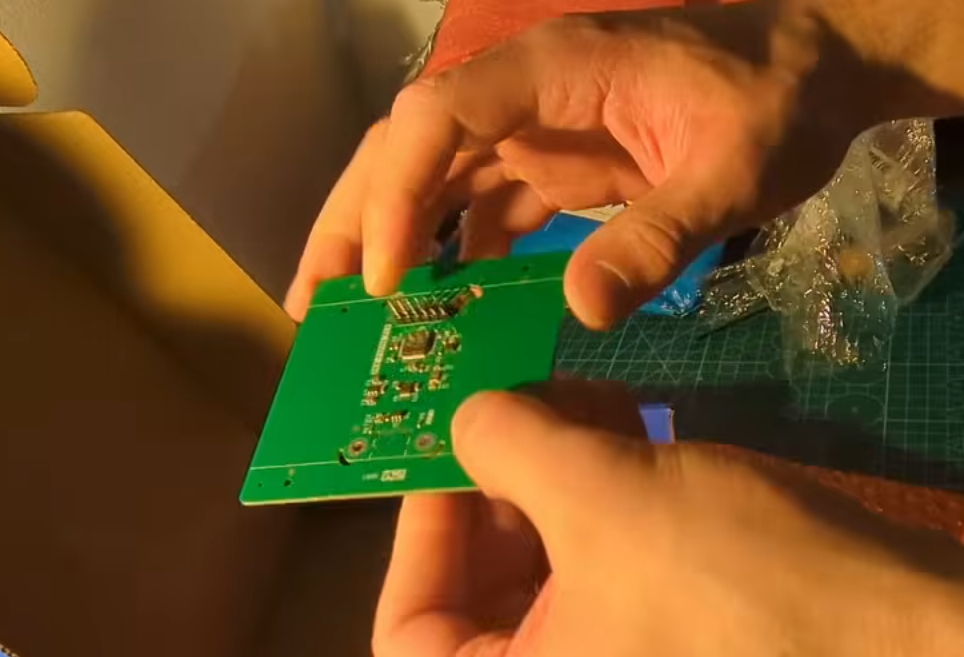
And it fits on a ~1x2in 2 layers PCB. Hereis the PCB out of the box :
You have to break the excedent fiber. I could’ve fit multiplt on a sigle 100x100mm plate but did not as it was my first run and didn’t really though about it in the moment.
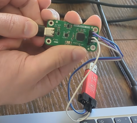
I cost me 100$ including PCB assembly and shipping. I had to solder USBC port and 6 pin header myself.
Software
Github link to software : https://github.com/0BAB1/tutorial-snippets/tree/main/14%20Noob%20tries%20Custom%20MSPM0%20PCB%20
To load the software, we fist have to get access to the MSPM0 SoC with a debugger.
Becaus eI did not use phil’s technique, I will plug a standard cheap STLINK V2 clone (~2-3€ on aliExpress) that support SW Debug.
And then we can use the following GDB/OpenOCD stack that can adapt to any target, to transfer your compiled binaries from any IDE to the said target:
1
C code + GCC (CCstudio to compile) -> GDB (gdb-multiarch) -> OpenOCD (with configs for our stack) -> Debugger (STLINKV2) -> SWD -> on chip Debug tap (full SoC access)
And then use GDB to load and debug the program easily with 0 IDE locked tools.
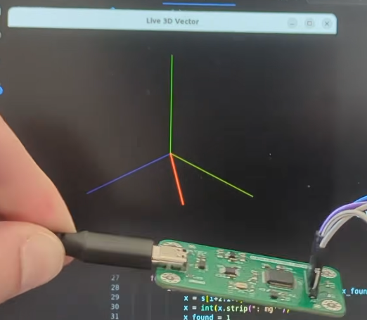
The sofware I made simply reads the I2C accelerometer data (acceleration over X,Y and Z) and then outputs it via UART.
I made a small python script that parses this UART data and displays it as a nice looking vector… Very nice !
Thank you for reading to this point. You can write a comment below if you have any question.
Godspeed
-BRH