Running DOOM on the HOLY CORE (Homemade CPU)
Introduction
Long story short, I made a CPU, the HOLY CORE. It is pretty simple yet pretty mature.
At some point, I wanted to take the whole thing a step further, as I implemented MANY features (check the DOCs for more infos) but how good are these features when I can’t really show what it does ?
I mean, implementing a simple single cycle CPU is something many people did to add that little resume claim, and there is no wrong in that, I do encourage it in fact. Yet I needed a demo that showed what happens when you take things far enough.
Because there is a HUGE difference between a demo simulated CPU and a real CPU. Mine isn’t even real ! It’s running on FPGA, some even TAPEOUT their CPU but I’d need some money to do that, which I don’t really have.
So I though for a moment until a friend of mine told me “but does it run DOOM ?”.
That’s it ! I needed to run DOOM !
Running DOOM is indeed the NUMBER 1 proof of concept I could have for this funky project.
So I did run DOOM and made a youtube video on the subject that got a fair amount of attention:
First Proof of Concept
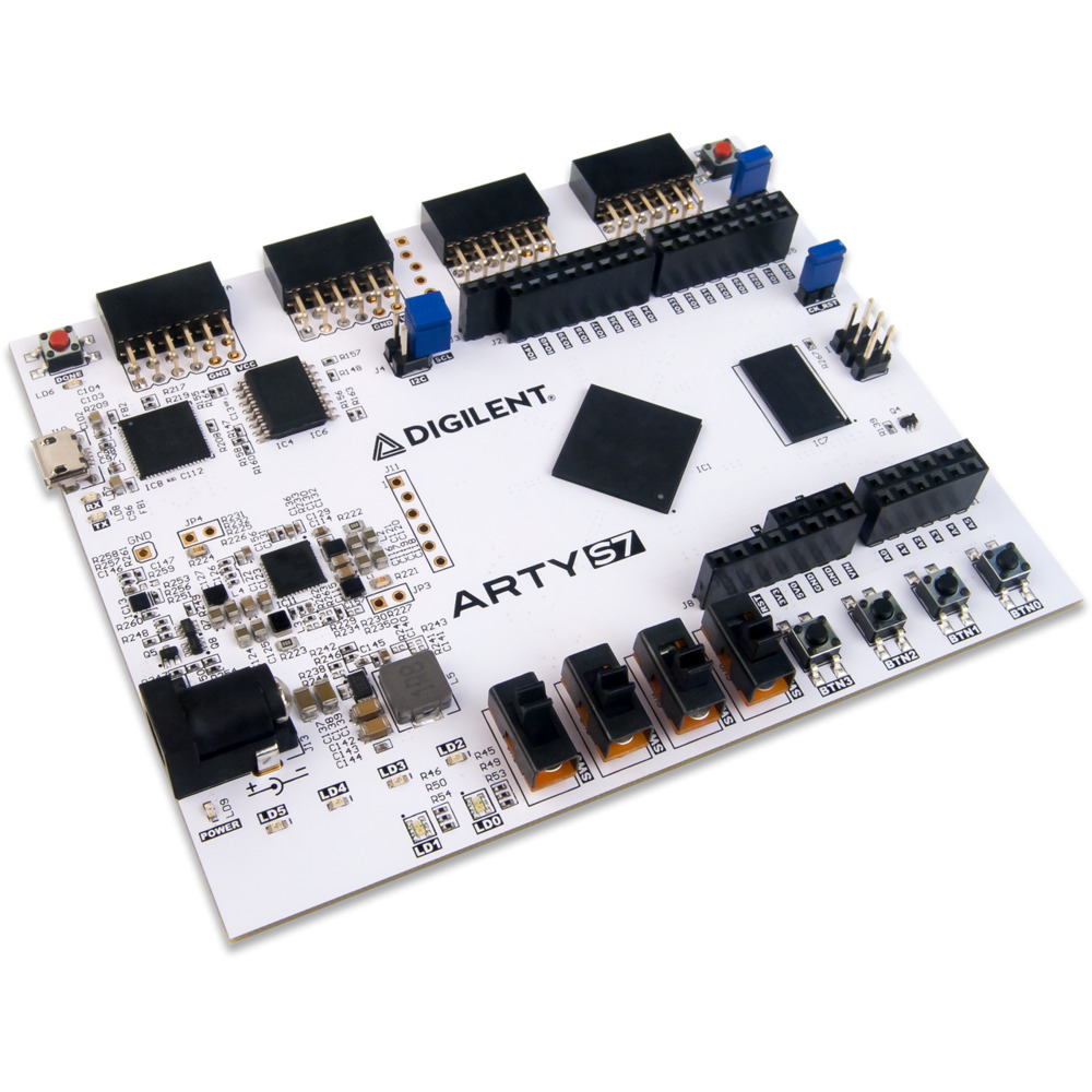
The whole thing runs on a ARTY-S7 board, embedding a SPARTAN7-50 FPGA (to run the CPU logic @30MHz), some DDR3 RAM (very handy to store big programs because the FPGA’s BRAM quickly limits projects that need some memory) and many GPIO pins, which is exactly what I needed to add an external screen.
At first I did n ot have a screen, so as a proof of concept (and after many hours of finding the remainings software AND hardware bugs), I used UART to render the frames. It was terribly slow but this prooved the project was doable and that frame were being rendered !
Running DOOM but for Real
Once the PoC was running, I ordered a small SPI screen. I selected it by searching online for arduino / raspberry gaming project where people ran games on external screen and went for a TFT 2.8” screen, which costs 9€ on amazon and 6-7€ on aliexpress. It also offer touch screen options, which I though could be nice for future projects.
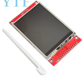
The screen itself does really matter, what really counts is the screen drivers chip whith which my CPU will interact via SPI, this screen is ILI9341 based.
So now, we have a screen, user inputs, AND we did a massive x8 on FPS, going from 0.25 FPS to a whopping 2 FPS! (including screen refresh time, which really tanks performance!).
Now let’s get a bit technical… Here’s a little list of the improvement I made to reach such “impressive” and “playable” performances :
HARDWARE PERSPECTIVE
The way I did that was simply by adding caches. A very small one for instructions (64 words i.e. 256KB but reads are instant which takes lots of FPGA resources) and a bigger one for data (1KB to 4KB but not much perf improvement between the two, but I can make it big as it is implemented as FPGA BRAM as read is synchonous, which makes this cache veeeery cheap resource-wise on FPGA).
The caches already existed but were very bad. I added them just to get good with AXI and did not think much about performances back then.
But now, after FIGHTING LIKE HELL to debug them and make them flexible enough to fit the needs of any piece of software, they are huge performance savers !
Judge by yourself ! here is a performance comparison between the different caches designs I explored (simulation):
| Metric | No Cache | Shitty I$ Only | Shitty D$ | Better D$ | Test I$ as D$ | FINAL D$ + OPTIMIZED I$ |
|---|---|---|---|---|---|---|
| Cycles | 1,000,000 | 1,000,000 | 1,000,000 | 1,000,000 | 1,000,000 | 1,000,000 |
| Instructions Executed | 164,817 | 355,014 | 20,561 | 689,260 | 455,031 | 846,829 |
| I Stalls | 808,339 | 194,098 | 137,074 | 196,309 | 484,520 | 32,439 |
| D Stalls | 26,844 | 450,888 | 842,365 | 114,431 | 60,449 | 120,732 |
| D Stalls on RAM Data | 25,948 | 448,872 | 782,190 | 113,535 | 59,553 | 119,836 |
| CPI | 6.07 | 2.82 | 48.64 | 1.45 | 2.20 | 1.18 |
| IPC | 0.16 | 0.36 | 0.02 | 0.69 | 0.46 | 0.85 |
| I-Cache Stalls (%) | 80.83 % | 19.41 % | 13.71 % | 19.63 % | 48.45 % | 3.24 % |
| D-Cache Stalls (%) | 2.68 % | 45.09 % | 84.24 % | 11.44 % | 6.04 % | 12.07 % |
| RAM D-Cache Stalls (%) | 2.59 % | 44.89 % | 78.22 % | 11.35 % | 5.96 % | 11.98 % |
| Total Stalls (%) | 83.52 % | 64.50 % | 97.94 % | 31.07 % | 54.50 % | 15.32 % |
Note that D$ = Data Cache and I$ = Instruction Cache. “Test I$ as D$” means I used the newly made D$ as an I$. But because D$ uses BRAM (because it’s larger and I needed some space), it adds a cycle on each fetch (sync read), which is not ideal. To solve that I$ was then turned into a smaller but more efficient cache by using raw registers instead of an FPGA BRAM block, meaning it was pretty resource intensive but the async read nature of registers allow for a 0 delay fetch, which is crucial for instructions because are constantly fetched from narrow memory regions. Data on the other hand is fetched in separate moments in time from scarser memoryregions, so I needed more space to reduce the miss count, meaning going for BRAM was the obvious choice here.
And here are some real FPGA measurements / benchmark:
| DOOM FPS BENCHMARK ON FPGA | No Cache | Shitty I$ Only | Shitty I$ + Slightly Better D$ | FINAL D$ + FINAL I$ |
|---|---|---|---|---|
| Frequency (Hz) | 25,000,000 | 25,000,000 | 25,000,000 | 25,000,000 |
| Game Cycles / Frame | 91,504,889 | 44,462,400 | 18,634,352.00 | ~10,000,000.00 |
| Game Sec / Frame | 3.66 | 1.78 | 0.75 | 0.40 |
| Game FPS | 0.27 | 0.56 | 1.34 | 2.5 |
“Shitty” Caches refer to the old caches design I had before. On top of being pretty under-optimized, they were full of bugs and edge cases that broke any serious software application. Now this are thanksfully fixed.
In theory, without a screen, we could reach 4 FPS. My ILI9341 screen could go waaay faster, up to a point where it would be so fast we don’t notice it, but I’d have to write my own SPI hardware controller AND add some sort of DMA transfer logic, which I really don’t wanna do for now, as that’s a week or two depending on how hard design verification will be…
We could also make the data cache more efficient by turning it into a 4 ways cache (currently 2 way) but again, that takes time that I don’t really have.
An other nice way to improve FPS was to add a REAL hardware multiplication. Until now, multiplication was done through a software subroutine which is extremely bad as DOOM uses multiplication heavily in backend computations, and each mul instruction would call a function, which had to save context on stack, which is painfully slow especially because these are mostly memory accessing instructions which can create cache misses, and then we perform a soft mul (slow) an we then restore context… BRUH that was slow ! Using the FPGAs DSP, the mul instruction now takes 2 clock cycles i.e. the same time it takes for a single load on cache hit ! And because we use DSPs to run the mul, making it extremely cheap in LUT / FF resources on FPGA. I also added division support but divisions are a bit rarer and now take 32+3 cycles, which is not good but not bad either compared to software subroutines.
Note : the FPGA carrier board I use (artys7-50, which I love and recommend) has some DDR3 RAM in which the whole ELF file is loaded, so cache misses are expensive but fetching data is still fairly fast (the main cycles cost being AXI protocol overhead rn). If I ever tape this out as a chip, I’ll have to use SPI memory which would make the design slower unless I use a larger / more optimized cache system.
SOFTWARE PERSPECTIVE
Software is not really my thing, I tried to “optimize” some functon by just ditching them but it turned out to simply make the game bad looking without increasing perfs.
The only optimization that I ended up doing was getting rid of the meld screen effect (which took ages to compute… and that leaves that weird effect on the GUI texture at the bottm of the screen).
Getting the screen to run was no big deal either. ILI9341 drivers are common and using an LLM, I got working drivers for my platform almost instantly (took me a day to make it work with a toy example where writing drivers can take a whole week usually because I have to pilot both my SPI hardware driver AND the screen at the same time ! which is something an LLM can do way faster than me). Nevertheless it then took me 2 weeks of debugging to realise I was using my SPI wrong, that was not the LLM fault but it took me 5mins of reading the datasheet to realise my clocking was not right, which I would have seen instantly If I read the datasheet myslef instead of giving that job to an LLM, lesson learned haha !
User input is not hard either, just a couple of memory mapped registers reads in my SoC’s UART controler to check out if any new char arrived.
Also the CPU have to have a time reference for ticks, which mostly happen only in CPU that handles interrupt as they all come with memory mapped timers, so it was easy to just make the ticks work for me but if you want to do the same project with a small CPU, make sure you at least have a timer otherwise the game just won’t work. Small but important detail (important mostly because full interrupts support is WAY harder to implement than an actual CPU imo).
CONCLUSION + LINKS
Anyway, the result is still good enough for me, and it now has a place in my showcase section in the HOLY CORE’s (name of my CPU) docs: https://0bab1.github.io/HOLY_CORE_COURSE/showcase/
If you have any questions on how I got to this point, you can ask here or check out my YouTube channel, where I document the process: https://www.youtube.com/@BRH_SoC
Thank you for reading to this point. You can write a comment below if you have any question.
Godspeed
-BRH