Gigabit Ethernet, HOLY CORE + KC705
Introduction
Github link to code : https://github.com/0BAB1/simple-ethernet
I’d say I’m a normal guy, but I’ve always liked very stupid projects.
So I made a CPU, the HOLY CORE which has recently been cited in academic research work !
I ported its SoC to some basic FPGA boards:
- Arty S7-50
- Basys3
- Zynq Z7-20
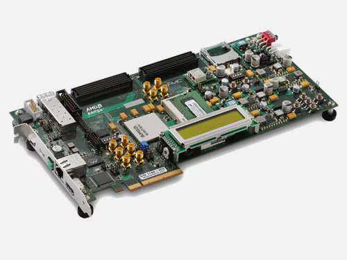
But today I decided to go at the KC705 and add ethernet functionalities to the system:
Motivation
I was frustrated not to understand ehternet, what is a MAC etc.. As always engineers love to make thing overcomplicated by using fancy acronyms to look good on linkedin.
So I took a week to implement it in my free time, I made my own MAC and documented the process ont youtube.
The Design
Overview
Let’s talk about the design with some exclusive insights:
It revolves around my HOLY CORE. The goal here is simply to exchange information with this homemade CPU via ethernet, as exmplained in the embedded video above.
Using my homemade CPU made things more dramatic for the video as well lol.
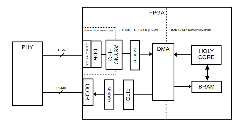
As you can see, the design is simple and complex at the same time.
First concern the FPGA I/Os, the IDELAYS2 are set to 0 so they are just tunable place holders depending on the PHY timings. Mine can be set to 0 and it will work just fine. Then an IDDR block, RGMII are PCB traces that carries the data, 1Bytes per clock rising edge. in GMII, each bit has its trace. RGMII aiming are reducing this trace count, we are left with 4 trace with a DDR rate to compensate. The IDDR block give us a clean byte at each rising edge we an use in fabric.
All datapaths in RX and TX chains (parser sender chains) are AXI Stream interfaces.
DMA
The data is made usable by the HOLY CORE using the xilinx’s DMA core and some BRAM. Nothing fancy, we’ll over that topic in more detail in the software part below.
Only hadware gotcha here is to get the adress space right. In the actual design there are 3 BRAMS to really separate adresses spaces.
2 BRAM to store the program (8kB eack) and 1 BRAM to store the DMA’s RX/TX buffers.
Clock domains
You may have noticed the RX part (before the parser) has its own clk domain. That is because the rgmii clock from phy is not reliable and we can’t run our entire fabric on it. Instead, we ensure this data enters or better real 125MHz clock domain unarmed using an async FIFO.
Once data arrives (from RX/parser), it arrives to the DMA core where it can get stored in the BRAM memory.
But…
The HOLY CORE runs at 25MHz and so does most AXI components like the BRAM.
it can run way faster on the Kintex7 FPGA. but i keept it at 25MHz because i was too lazy to test higher speeds and find the true limits by spamming design implementations.
So we have to cross these domain, in the schemes it is shown as the DMA handles it, in reality, the AXI4 interconnect handles this, but the idea is the same.
On the TX Side (sender), we get to send a GTX clock to the PHY chip, meaning we have the hand on the timing. So we can run all this logic on our main 125M fabric clock and pass the said clock along via GTX to the PHY chip. no CDC here.
Verification
Verification was done using cocotb, verilator and the cocotbect.eth etension.
It is giga simple, I did not do many assertions there. It is this kind of testbench where you just check visually that eveything is okay. As parser & sender logics revolve around simple FSM, I did not bother checking corner cases much.
Now this verification was a bit special, like all HIGH SPEED I/O designs that involves some IDELAYS and IDDR, you have to handle that differently in simulation when you are using a separate simulator.
Tjis is a gotcha that can reveal to be a bit of a pain, as you have to recreate the I/O mudiules behavior in specific simulator logic.
It works fine but you never know if your simulation is nailing it 100%, which is why using already proven open source code might be the best move herre
someting like this OODR implementation : https://github.com/alexforencich/verilog-ethernet/blob/master/rtl/oddr.v that depends on the target.
However I made my own wich depends on SIMULATION flag being set or not:
1
2
3
4
5
6
7
8
9
10
11
12
13
14
15
16
17
18
19
20
21
22
23
24
25
26
27
28
29
30
31
32
33
34
35
36
37
38
39
40
41
42
43
44
45
46
47
48
49
50
51
52
53
54
55
56
57
58
59
60
61
62
63
64
65
66
67
68
69
70
71
// rgmii_rx.sv

// ...
// port defs
// ...

// FOR COCOTB BEHAVIOR SIMULATION
`ifdef SIMULATION
    assign clk_125 = rxc;

    logic [3:0] rxd_rise, rxd_fall;
    logic       rxctl_rise, rxctl_fall;

    // rising edge => low nibble
    always_ff @(posedge rxc) begin
        rxd_rise   <= rxd;
        rxctl_rise <= rx_ctl;
    end

    // falling edge => high nibble
    always_ff @(negedge rxc) begin
        rxd_fall   <= rxd;
        rxctl_fall <= rx_ctl;
    end

    assign rx_data = {rxd_fall, rxd_rise};
    assign rx_dv   = rxctl_rise;
    assign rx_er   = rxctl_rise ^ rxctl_fall; // RX_ER = RX_DV XOR ctl_fall

// FOR KINTEX (KC705) synth
`else

    // we gather the clock in fabric using bufg
    BUFIO u_bufio (
        .I (rxc),
        .O (rxc_bufio)
    );

    BUFG u_bufg (
        .I (rxc),
        .O (clk_125)
    );

    logic [3:0]  rxd_delayed;
    logic        rx_ctl_delayed;

    // IDDR to capture falling and rising edges of rxd[3:0]
    logic [3:0] rxd_rise, rxd_fall;

    IDELAYCTRL u_idelayctrl (
        .REFCLK (clk200),
        .RST    (rst),
        .RDY    ()
    );

    genvar i;
    generate
        for (i = 0; i < 4; i++) begin : gen_idalye_two_rxd
            IDELAYE2 #(
                .IDELAY_TYPE           ("FIXED"),
                .IDELAY_VALUE          (0),
                .DELAY_SRC             ("IDATAIN"),
                .HIGH_PERFORMANCE_MODE ("TRUE"),
                .REFCLK_FREQUENCY      (200.0),
                .SIGNAL_PATTERN        ("DATA"),
                .CINVCTRL_SEL          ("FALSE"),
                .PIPE_SEL              ("FALSE")
            ) u_idelay_rxctl

    // ... rest of the logic
Software & Results
So to test this design, I and Claude.ai made a python TUI that sends ethernet packets acked with waveform samples.
The goal is to run an FFT an these samples and return the reult to the TUI.
The firmware leverages Xilinx’s DMA status and control to arm RX, know when a pcket arrive to run the FFT, copy the results in a TX buffer, and then tell the DMA to send it back:
1
2
3
4
5
6
7
8
9
10
11
12
13
14
15
16
17
18
19
20
21
22
23
24
25
26
27
28
29
30
31
32
33
34
35
36
37
38
39
40
41
42
43
44
45
46
47
48
49
50
51
52
53
54
55
56
57
58
59
60
61
62
63
64
// main.c

#include <stdint.h>
#include "holycore.h"
#include "holy_core_soc.h"
#include "fft.h"

#define DMA_BASE         0x10040000
#define DEBUG            0

#define MM2S_DMACR      (*(volatile uint32_t*)(DMA_BASE + 0x00))
// other defines or DMA regs

#define DMA_RX_BRAM     0x80004000
#define DMA_TX_BRAM     0x80005000
#define EXPECTED_POINTS     256
#define EXPECTED_FFT_POINTS 128

// FFT working buffers — static so they don't go on the stack
static int32_t fft_re[FFT_N];
static int32_t fft_im[FFT_N];

void main() {
    uart_puts("\n\r[BOOT] DMA ethernet FFT starting\n\r");

    int32_t* rx = (int32_t*)DMA_RX_BRAM;
    int32_t* tx = (int32_t*)DMA_TX_BRAM;

    while(1) {
        // ===== ARM RX =====
        S2MM_DMACR = 0x00000004;
        while(S2MM_DMACR & 0x00000004);
        S2MM_DMACR  = 0x00000001;
        S2MM_DA     = DMA_RX_BRAM;
        S2MM_LENGTH = 1500;

        // ===== WAIT FOR PACKET =====
        while(!(S2MM_DMASR & 0x1000));
        S2MM_DMASR = 0x1000;

        // ===== LOAD INTO FFT BUFFERS =====
        // scale input from int32 to Q1.15 range to avoid overflow
        for (int i = 0; i < FFT_N; i++) {
            fft_re[i] = rx[i] >> 16;   // scale down int32 → Q1.15 range
            fft_im[i] = 0;
        }

        // ===== RUN FFT =====
        fft(fft_re, fft_im);

        // ===== COMPUTE MAGNITUDES INTO TX =====
        fft_magnitude(fft_re, fft_im, tx);

        // ===== SEND =====
        MM2S_DMACR = 0x00000004;
        while(MM2S_DMACR & 0x00000004);
        MM2S_DMACR  = 0x00000001;
        MM2S_SA     = DMA_TX_BRAM;
        MM2S_LENGTH = EXPECTED_FFT_POINTS * sizeof(int32_t);

        while(!(MM2S_DMASR & 0x1000));
        MM2S_DMASR = 0x1000;
    }
}
For simplicity of interaction with MMIOs and SoC interface witing, HOLY CORE internal caches are disabled and only the AXI LITE interface is used to poll DMA and exchange data with the BRAMs:
.section .text
.global _start

_start:
    la t0, startup_code
    csrw mepc, t0
    mret

startup_code:
    la sp, _stack_top     // Set stack pointer

    # Setup uncached addr range : DISABLED
    li t0, 0x00000000
    li t1, 0xFFFFFFFF
    csrrw x0, 0x7C1, t0
    csrrw x0, 0x7C2, t1
    csrrw x0, 0x7C3, t0
    csrrw x0, 0x7C4, t1

    call main             // Call main
    j .                   // Infinite loop if main returns
Because yes, My HOLY CORE has runtime configurable caches, pretty cool right ? yes I’m flexing.
softwre is available in HOLY CORE’s exmaples : https://github.com/0BAB1/HOLY_CORE_COURSE/tree/master/3_perf_edition/example_programs/ethernet_dma
Anyway, here is the final result:
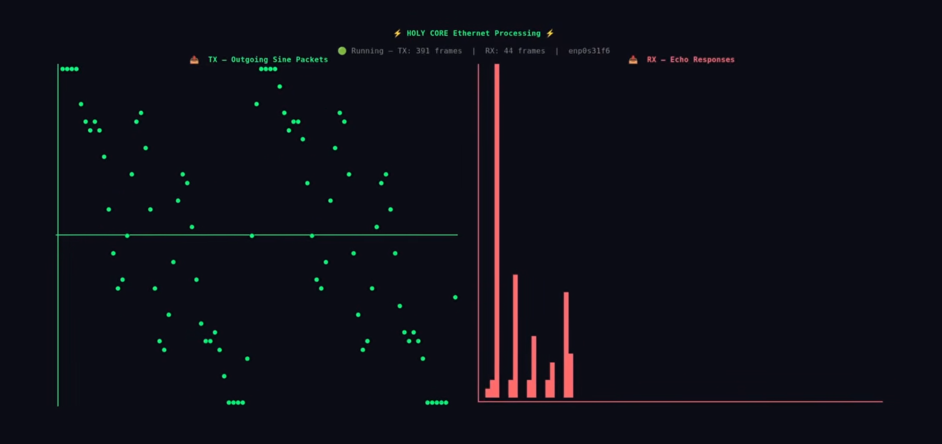
On the left, the generated waveform samples. On the Right, FFT result comming from the HOLY CORE.
Improvements to Come
There multple little problems. FIFO solve most of them but still, there is this corner case where you arm the DMA as data is being streamed. If the fifo is full (which may happen as the CPU is slower). you may get dumb data. A FIFO tailored to ethernet frames needs (i.e it only assert tvalid on complete frames and drop old stale frames entirly when full) would be appreciated for such a design.
Also, CRC is not check on the RX part. At these scales (the main pc being 20cm away from the board) we can assume that but a CRC check won’t hurt and is not that hard to add (I had to add it for the TX part, so I was just to lazy to add a check on RX parser.)
Thank you for reading to this point. You can write a comment below if you have any question.
Godspeed
-BRH